|
|
|
|
In order to achieve efficient operation of a sequential digital system, the timing of the clock used by the storage elements in a complex VLSI system must be as close to ideal as possible. In order to achieve high accuracy, today’s clocking subsystems typically use off-chip crystal oscillators. These oscillators are based on a piezoelectric crystal, electrically equivalent to an LRC circuit, Figure 1. If such element is included in reactive feedback of a non-linear amplifier, the conditions necessary to establish the oscillations are satisfied only in a narrow frequency range where the reactance of the quartz oscillator is positive. This frequency range, and the frequency of the oscillations are determined only by the properties of the crystal. The Q-factor of such circuits is typically very large, resulting in very small variation of resonant frequency (a few parts per million).
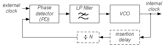
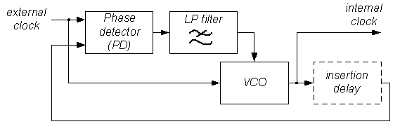
Figure 1. Crystal oscillator equivalent circuit Neither frequencies practically achievable by the crystal oscillators nor the bandwidth of the chip I/O pads exceed several tens to hundreds of megahertz. In addition, on-chip clock distribution typically requires several levels of amplification, implying large latency between the input clock and the clock used by the storage elements. Therefore, if an off-chip clock is used directly on chip, the on-chip circuits would operate in asynchrony with the off-chip circuitry and the system synchronization would be lost. For these reasons, the low-frequency high-accuracy clock is brought on chip and used as a reference for a phase-locked loop (PLL) or delay-locked loop (DLL). Phase-locked loop, shown in Figure 2, consists of phase detector (PD), low pass filter, and voltage-controlled oscillator (VCO), output of which is fed back to the phase detector. In addition, PLL may contain a frequency divider in the feedback to the phase detector PD. This frequency divider allows for generation of a high-frequency on-chip clock signal in phase with low-frequency off-chip clock. Typically, a copy of the clock distribution path is included into the PLL feedback, which ensures that the internal clock is in phase with the external system clock, Figure 2. Delay-locked loop (Figure 3) has similar structure to PLL. It consists of a phase detector (PD), a low-pass filter (LP), and a voltage-controlled delay line (VCDL). The output of the low-pass filter controls the delay of VCDL, for example by changing its supply voltage, capacitive load, or the conductance of the driving transistors. DLL adjusts the delay of the VCDL so that the signal at its output is aligned with the input clock reference. It cannot be used as frequency multiplier, as the output signal is a simple replica of the input reference.
Figure 2. Diagram of phase-locked loop (PLL)
|
|
|
|