|
|
|
|
Clock Timing ParametersThe clock waveforms are shown in Figure 1. The timing parameters of the clock signal are:
Multiple-phase clocks are characterized by overlap V, which is the fraction of the clock period where the active levels of the two phases (presumed high) are overlapped. Consequently, multiple-phase clocking can be overlapping or non-overlapping. The most widely used multi-phase scheme is non-overlapping two-phase scheme [Unger1986].
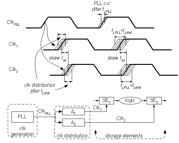
Figure 1. Clock timing parameters Clock Timing Non-idealitiesThe non-idealities of clock generation and clock distribution system manifest themselves as uncertainties of the clock edge arrivals around nominally defined time instances. The examples of the clock timing non-idealities are phase error of the clock generator, load mismatch at any two nodes of the clock distribution tree, and process, voltage, and temperature variation. Two modes of the uncertainties are typically defined: peak-to-peak (p-p), or long-term, and cycle-to-cycle (c-c). Peak-to-peak uncertainty represents the absolute boundaries of the clock uncertainty in long-term operation. Cycle-to-cycle clock uncertainty is the maximum uncertainty between two consecutive clock edges. If defined for a clocking subsystem, cycle-to-cycle clock uncertainty is more useful parameter, as it provides more relaxed timing constraints that presents actual impact of the clock uncertainties to the cycle time. It is also helpful to define short-term clock uncertainty (cycle-to-Nth-cycle clock uncertainty) as the uncertainty between two clock edges within several adjacent cycles. This definition allows us to account for the accumulating property of the clock generator jitter in the timing analysis of the systems where exists an interdependence between data arrivals from several clock cycles. Two types of clock timing non-idealities are commonly distinguished. First, commonly referred to as clock jitter, presents temporal uncertainty of a clock edge at a single point of clock termination – storage element, clocked logic gate etc. As shown in Figure 2, both clock generation and clock distribution system are sources of clock jitter. Second type of clock uncertainty, clock skew, describes spatial uncertainty between two different clock termination points (storage elements, clocked logic gates etc). Simplified, it is considered to be a function of clock distribution system only. However, this is not true if a distributed clock generation is employed. Clock jitter and clock skew are illustrated in Figure 2, where the timing is depicted with respect to the first rising edge of the PLL clock ClkPLL. The difference between the arrival of two concurrent edges of the clocks Clk1 and Clk2 occurs due to the delay difference between the two paths through the clock distribution network. This difference has two components: “static”, or clock skew, and variable, or clock distribution jitter. Compared to this uncertainty, clock uncertainty between Clk1 and Clk2 in two consecutive cycles is augmented by the clock generator jitter, as shown in Figure 2.
Figure 2. Components of clock uncertainty
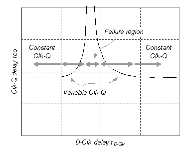
Timing Parameters and MetricsIn order to be able to quantitatively express performance of a flip-flop and compare one flip-flop to another, one must define the timing metrics. The main criterion used to define timing metrics of the flip-flops should be the time that the clocking takes away from the clock cycle for pipeline synchronization, or the timing overhead of the clocking strategy. The goal is to maximize the portion of the clock cycle that is left to the logic for useful computation. In this way, a storage element with smaller timing metric eventually allows more time for logic computation, which is a feature that defines the performance of a clocking strategy. A simple inspection shows that the time the clocking strategy takes away from the clock cycle is the sum of the clock-to-output of the releasing flip-flop, setup time of the receiving flip-flop, and the clock uncertainty. Since the clock uncertainty is a characteristic of system design, it can hardly be controlled by flip-flops. For this reason, the clock uncertainty is not considered a part of the timing metric. Thus the timing overhead of the clocking strategy based on the flip-flops is the sum of the clock-to-output of the releasing flip-flop and the setup time of the receiving flip-flop. In Chapter 4, it will be shown how the effect of the clock uncertainties to the timing of the flip-flops can be characterized. In order to provide more precise understanding of the timing metric, we examine the definition of setup and hold times of the flip-flops. If an experiment is conducted to measure the degradation of clock-to-output delay (tCQ) of a flip-flop as a function of data-to-clock delay (tD‑Clk), resulting characteristics typically looks as shown in Figure 3. When tD-Clk is large enough, tCQ is constant. As the data arrival approaches the capturing clock edge, a degradation in clock-to-output time occurs, i.e. the output of the flip-flop arrives later than in the nominal case. If the data arrival is pushed even further, the degradation eventually becomes severe enough to cause the capture to fail. This failure is seen as the violation of the setup requirement. The exact setup time position on the x-axis is somewhere between latest data arrival for the constant clock-to-output time and the failure.
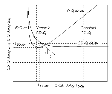
Figure 3. Clock-to-output characteristics of flip-flop If the data arrival is set long enough after the clock arrival, the previous data is safely captured in the flip-flop (e.g. if the data transition is zero to one, zero is captured). As the data arrival approaches clock edge, the clock-to-output time starts to degrade in a similar fashion as from the setup side. If the data arrives early enough, this degradation is so severe to cause the transition to fail. This scenario corresponds to the violation of the hold time requirement. The exact position of the hold time is somewhere between the earliest data arrival for the stable clock-to-output time and the failure. Most common approaches define timing parameters of a flip-flop based on the signal integrity criteria. For example, setup time and hold time are defined as the points where some critical internal node experiences (unwanted) glitch of defined magnitude – e.g. 10%VDD, 0.2V etc. This approach binds the definition to a design-specific node, which disallows a fair comparison of different storage elements. In addition, the definition is imprecise – defined threshold may be far non-critical for some flip-flops, while it may cause severe internal signal degradation for others. Other approaches define setup and hold times at points where the clock-to-output characteristic experiences the degradation equal to some defined percentage of the nominal clock-to-output delay. Compared to the definition based on a glitch, this definition is universal, and thus better to some extent. However, it is unfair as it relates the definition to the nominal clock-to-output time, so that different degradations are allowed for the designs with different nominal delays. In addition, the specification of delay degradation percentage is vague. As an alternative to these signal integrity criteria, in the following sections we discuss the definition of the timing parameters based on achieving maximum performance. Setup Time, Data-to-Output DelayAccording to the setup requirement, the sum of the worst-case clock-to-output time of the releasing flip-flop, worst-case logic delay and worst-case setup time of the receiving flip-flop has to be less than or equal to the clock period T. Assuming that the flip-flops are of the same type, the two flip-flop parameters can be merged into a single parameter, called data-to-output time (tDQ), expressing the delay from the data input to the output as a function of the data-to-clock delay:
Figure 4. Data-to-output delay characteristic The data-to-output characteristic based on the clock-to-output characteristic from Figure 3 is shown in Figure 4. In order to maximize the time given to the logic computation, the goal is to operate at the minimum point, tD-Clk=tSU,opt, Figure 4. In the region of variable Clk-Q delay, the incremental benefit obtained when the data arrival is delayed is degraded by the increase in clock-to-output time. As long as the improvement obtained from reducing tD-Clk are greater than diminishing effect of tCQ degradation, it is beneficial to delay the data arrival. Consequently, the optimum point on the clock-to-output characteristic is at the slope of 45°, i.e. at the point where the benefits from reducing tD-Clk are equal to the degradation of tCQ. More formally, the optimum point can be found if the derivative of Eq. (1) is taken with respect to tD-Clk and forced to zero:
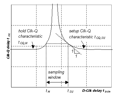
The minimal value of the data-to-output delay is referred to as minimum data-to-output delay (tDQ,min) and the data-to-clock delay corresponding to this point is called optimal setup time (tSU,opt) [Stojanovic1999]. This optimal setup time provides the performance-based definition of the setup time of the flip-flops. The minimum data-to-output delay is the smallest timing overhead of a flip-flop. Using the data-to-output representation of flip-flop delay is not only important for timing characterization and optimization, but it is also essential in design of high-performance systems using clock uncertainty absorption and time borrowing. Hold Time and Internal Race ImmunityAn early data arrival has to satisfy the hold time requirement of the receiving flip-flop. The question of which point on the clock-to-output delay characteristic satisfies this hold requirement is similar to that of the setup time. The answer to this question depends on whether t he criterion is based on the signal integrity or the performance. If the hold time is defined based on the signal integrity, it is determined upon the same criteria as for the setup time. In case of performance-driven definition of timing parameters, we observe that, prior to hold time violation, an early data arrival to the receiving flip-flop causes an increase clock-to-output delay data capture from the previous cycle, Figure 3. Therefore, data arriving too early to the receiving flip-flop may corrupt the timing in the subsequent stage in which the flip-flop releases data. This subsequent stage may contain slow paths that are designed just to meet cycle time with worst-case clock-to-output delay and setup time. Thus, in order to keep the timing uncorrupted, the data is allowed to arrive any time later than the point where the clock-to-output delay is less than or equal to the clock-to-output delay observed at the setup time. The slope of the characteristic at the hold time is not specified, i.e. it does not have to be 45°. The above observation provides the definition of the hold time: if tCQ(tD-Clk) is the clock-to-output characteristic of the flip-flop, divided into set-up (tCQ,SU(tD-Clk)) and hold (tCQ,H(tD‑Clk)) regions, and tSU,opt is the optimal set-up time, then:
In Eq. (3), tCQ,SU(tD-Clk) is the setup part of the clock-to-output delay characteristic, and tCQ,H(tD-Clk) is the characteristic of the previous data capture, Figure 5. As the timing requirement for the fast paths suggest, timing parameter of a flip-flop that depicts the robustness to the fast paths is the difference between minimum clock-to-output delay and maximum hold time, defined as the internal race immunity (IRI, [Markovic2001]):
The internal race immunity is the fast path safety margin of the pipeline stage with same releasing and receiving flip-flop, without logic between flip-flops and without clock uncertainties. If the internal race immunity is negative, extra delay has to be provided to force data arrival time of the receiving storage element into the stable region. For the safe operation without logic between flip-flops, the internal race immunity must be higher than the maximum clock uncertainty between releasing and receiving flip-flop.
|
|
|
|