|
|
||
07/02/04 |
|
|
Addition is often on the critical path of modern day microprocessor. Adder is also the “hot spot” among all other execution units in a processor core. Thus, a fast and energy-efficient adder is essential to a high-performance microprocessor. Implementing fast addition has been an important subject since the 1950s. Ripple Carry adder is the first and the most fundamental adder that is capable of performing binary number additions. Since its latency is proportional to the length of its input operands, it is not very useful. Weinberger and Smith have made the first major break-through in speeding-up additions by proposing the well-known scheme, Carry Look-ahead adder [1]. Rather than rippling carries throughout the adder, it uses parallelism to propagate carries much quickly.
Nowadays, implementing addition has becoming more and more challenging.
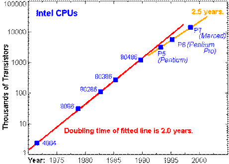
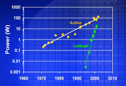
Current trend of microprocessor development continues to follow Moore’s Law,
shown in Figure 1. As a result, the clock frequency of microprocessors
doubles every two years and rapid increase in power consumption is also
observed as shown in Figure 2. Thus, to have a higher performance design yet without
having too much penalty on power consumption, changes at all levels are
required.
Figure Moore's Law Trend
Figure Power Trend [Gordon Moore, ISSCC 2003]
There are several levels of hierarchy one can improve addition operations. First it can be improved at architecture level. By using an algorithm that incorporates a faster carry propagation method such as prefix tree adder schemes, addition time can be reduced. By adding clock gating and sleep mode, power can be saved when the adder is not in use. Multiple power supplies can also be used to supply lower voltage to less critical paths in order to reduce power. For mobile applications, dynamic voltage scaling is a widely used technique to reduce power consumption. It automatically optimizes the supply voltage and the operation frequency for a given workload. To reduce the addition latency and power, one can also improve it at circuit level. For example, selecting dynamic logic over static CMOS logic would improve the speed of operation. Transistor sizing can be used to improve speed and power. A transistor sizing tool parameterizes the sizes of transistors in a circuit based on circuit characteristics such as driver size, load, supply voltage, operating temperature, and etc. After completing a transistor level design, the customized cell placement can be used, which may produce a better layout than automatic place and route tool. With today’s advanced technology, a careful planning of wires and cells before placement is often necessary in achieving a better timing and power. Finally, speed can be improved at process level. A more advanced process technology can be used. This could be scaling the transistors’ feature size, using copper interconnects rather than aluminum interconnects, using SOI (Silicon on Insulator) CMOS technology rather than Bulk CMOS technology, using thinner and higher K dielectric insulator as gate oxide, etc. |
Copyright Advanced Computer Systems Engineering Laboratory, 2004
This site was last updated 04/27/04