![]()
|
|
|
|
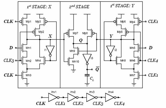
The Symmetric Pulse Generator Flip-Flop (SPGFF):The Symmetric Pulse Generator Flip-Flop (SPGFF) was developed here at ACSEL by Nikola Nedovic [6]. The SPGFF is the DETFF of choice for this project. It is a simple two stage flip-flop shown in Figure 1. An advantage of this flip-flop is that it consists of only two fast stages: the first a dynamic stage and the second a simple static NAND.
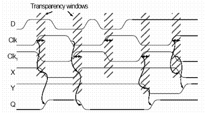
Figure 1 - SPGFF Pulse generating stages X and Y of the flip-flop work in the opposite phases of the clock: when clock is high, node Y is pre-charged and node X holds the value captured at the rising edge; when clock is low, node X is precharged and Y holds the value captured at the falling edge. The output stage selects between X and Y. Figure 2 shows the operation of the SPGFF. The principle of operation is as follows. As shown is Figure 2, node X is precharged high during the time when the clock CLK is low. When CLK makes a low-to-high transition, X is allowed to conditionally evaluate to low through transistors Mn1, Mn2, Mn3, depending on the level of input D (if D=0, X stays high, otherwise it switches low). Node X is allowed to switch to a low level only in the short time-window following the rising clock edge. This time window is defined by the delay of three inverters Inv1-Inv3 (Fig. 1). This feature makes the set-up time of the storage element negative and the short transparency window makes clock uncertainty absorption possible. After the transparency window elapses, the value of X is preserved while the clock is high, by inverter I1 and transistors Mp2, Mp3, Mn3 and Mn4. Node X is again precharged high after the falling edge of the clock CLK. Thus, node X is allowed to switch from high to low only shortly after the rising edge of the clock and from low to high only after the falling edge of the clock. This ensures that the transitions of the output Q or Q are also synchronous with the clock edges.
Figure 2 - Timing diagram of the SPGFF The evaluation and precharge phase of node Y are interchanged with respect to those of node X. Node Y is precharged high during the time CLK is high and node CLK1 is low. It is then allowed to evaluate only after the falling edge of CLK, during the time window determined by the propagation delay of Inv2-Inv4. Thus, the two first stages of the flip-flop alternately capture the data value D. At any moment, the sampled value of D at the most recent clock edge is held at either node X or Y, while the other of X and Y is precharged high. Since the second stage of SPG-FF is a static NAND gate (transistors Mn9, Mn10, Mp7, Mp8), Q takes the value X when CLK is high (Y=1), and Y when CLK is low (X=1). Thus, at any moment, Q takes the value of D sampled in the most recent transparency window. Adding Functionality:For the practical use of DET-CSEs in designs, functionally enhanced DET-CSEs need to be explored. Any functionality added to the DET-CSE will increase its power consumption. This power consumption cannot be significantly larger than its SET-CSE counterparts if the use of DET-CSE as a low power technique is to be proven. The addition of scan to CSE increases area, power, and possibly has the largest impact on performance, so it will be investigated first. Scan:The complexity of designs
today make design-for-test a necessity. This requires clock storage elements
with scan capability. Unfortunately, adding scan capability can greatly increase
power consumption of the CSE. Studies have reported as much as 50% increase in
power of a scannable design over that of a non-scannable design. |
|
|