
![]()
|
|
|
|
Digital System PerformanceA common performance metric in digital synchronous systems is the maximum clocking frequency of the system. Although such a metric does not take into account the ammount of "work" done during this clock period, for our design it is a meaningful measurement, since the two implementations perform the same function. Thus, to analyize the performance trade-off of a design implementing DET-CSEs it is necessary to accurately measure the impact on the maximum clocking frequency of the design. DET-CSEs have different timing parameters than SET-CSEs. In digital synchronous systems the critical timing constraints of the design are that the critical path and critical race logic delay paths must not violate the timing parameters of the clocked storage element. Figure 1 shows a model of digital synchronouns system timing which is typically described with a "launching" clocked storage element, a "receiving" clocked storage element, and the logic function in between. All logic paths in a synchrous system can be modeled as shown in Figure 1. 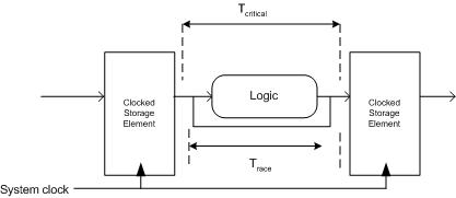 Figure 1 - Synchronous digital system timing
The timing parameters for clocked strage elements are the set-up time,
hold-time, and clock-to-output delay time. For SET-CSEs these parameters are
given for the active edge. DET-CSEs have timing parameters for both clock
edges. These parameters are shown in Figure 2.
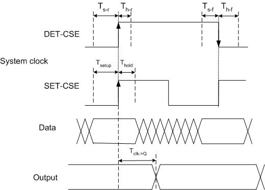 Figure 2 - Clocked Storage Element timing
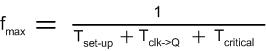
parameters In a SET-CSE digital synchronous system the maximum
clocking frequency is given by equation 1 (ignoring clock uncertainty). Another useful way to think of the set-up and
clock-to-output timing parameters is to view it as the total delay through the
clocked storage element, or the total timing overhead introduced by the clocked
storage element. This is the total time taken away from useful logical function
time due to the use of the clocked storage element as a synchronization device.
For a DET-CSE digital synchronous system the maximum
clocking frequency is determined by the timing parameters for each edge. The
timing parameters yield a minimum high and low clock width constraint (equation
2 and 3), which together form the maximum clocking frequency for a DET-CSE
synchronous system (equation 4 - these equations ignore clock uncertainty).
Equations 2-4 imply that the optimal clock duty
cycle is a function of the timing parameters for each edge, and can be expressed
as shown in Equation 5.
|
|
|
 equation (1)
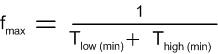 equation(5)
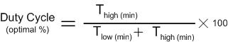 equation(6)