
![]()
|
|
|
|
ApproximationsA first order approximation of the power consumption of the design is performed by applying blanket toggle rates to all nodes in the netlist of the SET-CSE design. This gives us a ball-park idea of the power consumption in various components of the design, and the expected savings of a DET-CSE design. Although this first-order analysis provides some insights into the power consumption of the logic gates, memories, and clocked storage elements, it does not give a good indication of the power consumption in the clock tree distribution network. The netlist, output from synthesis, treats the clock node as an ideal node with infinate drive. Thus, the wiring needed to balance and route the clock, as well as the buffers needed to drive the clock throughout this network is not accounted for. To account for a real clock tree distribution network, an estimate of the total loading of an H-tree distribution network had been derived by previous research at ACSEL conducted by Nikola Nedovic. The equation given below is a derived estimate of the total capacitance in an H-tree clock distribution network, based on fan-out of four (FO4) rules. 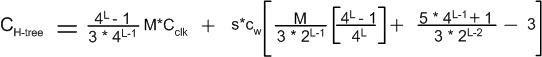 equation (1)
equation 1 definitions:
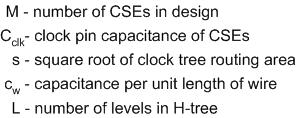 The M*Cclk term is the total loading of the clock net due to the CSEs in the design. This term can be taken straight from the netlist results. The s*cw term can be calculated based on the total area reported by the synthesis results minus the "non-routable" area (i.e. memory cells, or other macros). A capacitance per unit lenght of wire to be used is 0.2fF. The number of levels in the H-tree should ensure that the leaf buffers are not driving too big of a load (i.e. also around FO4). Incorporating equation 1 for the capacitance of the H-tree, an equation for the total power of the H-tree is derived and shown as equation (2).  equation (2)
equation 2 definitions:
 The summation term in equation 2 is the total power consumed by the clock buffers when switching. The Energy of the clock buffer is a parameter that is easily obtained from any standard cell technology library. The results of this approximate power estimate will be posted in the results section of the Project web-page when available. More accurate Power analysisA more accurate power analysis of the design can be obtained by linking in
toggle rate data from simulations and applying them to the design. The toggle
data can be a testbench simulation (which probably does not reflect nominal
operation of the design), or simulations running a sequence of instructions on
the design (e.g. a piece of benchmark code). A simplified tool flow for this
method is show below in Figure 1. 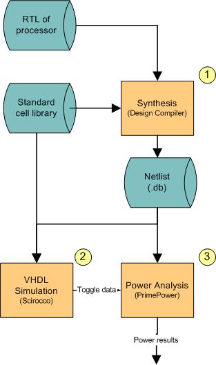 Figure 1 - Simplified tool flow for power analysis with toggle data Details of Tool flow
Power savings of DET-CSE designAs mentioned previously, the power savings of the DET-CSE design is
acheived by running the design at a lower clock frequency (half the SET-CSE
clock frequency) thereby reducing the power consumed in the clock
distribution network. Equation 1 gives an expression for the total
switching capacitance in the clock distribution network. The first term in
equation one is the total switching capacitance due to clock storage element
loading, and the second term is due to clock distribution network wire
loading. For the case where M >> 4^L >> 1 the two terms can be approximated
as shown in equatin 3 and 4.
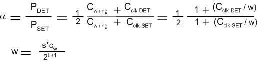 equation
5 and 6 equation
5 and 6
w is the the average capacitance of the wire needed to route the clock
throughout the entire hierarchy of the clock distribution network.
Figure 2 shows is a plot of the power ratio alpha versus the loading of
the SET-CSE device. In the case where the loading of the clock tree is
dominated by the wiring capacitance, or where the loading of the DET-CSE
and SET-CSEs are close, the DET-CSE design saves 50% of the power
consumed in the clock tree (i.e. alpha = 0.5). As shown, DET-CSEs offer
power savings even for designs where wire capacitance does not dominate
and there is a significantly higher loading for the DET-CSE.
|
|
|