
![]()
|
|
|
|
ArchitectureThe LEON2 processor is a synthesizable VHDL model of a 32-bit SPARC V8
processor architecture. The full source code is available under the
GNU LGLP license. For more details go to
www.gaisler.com/leonmain.html In our design the LEON2 Processor is configured with the following features:
Figure 1 shows the Architecture of our design of the LEON2 Processor. 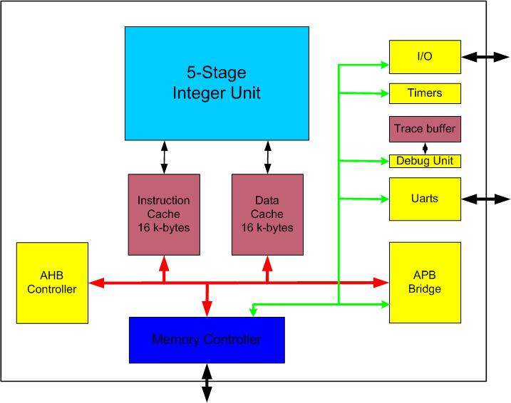 Figure 1 - Leon SPARC V8 Processor Architecture and Configuration DET-CSE Implementation IssuesThere is one clearly evident problem with implementing DET-CSEs in the
architecture presented above, and is the case for any design requiring
access to blocks of memory. The concept of halving the clock frequency for
a design implementing DET-CSEs and maintaining the same performance runs
into problems when the design accesses memory arrays. Typically these
memory arrays are implemented as dense on-chip SRAM or ROM hard macros. In
a standard cell design, these would be the only clocked elements in the
design that are not some type of flip-flop or latch. Thus replacing all the
clocked storage elements in the design with DET-CSEs still leaves the
problem of how to deal with the memory macros. By halving the clock
frequency, the memory bandwidth would also effectively be halved. This
would certainly have a deleterious impact on performance and essentially
make the use of DET-CSEs a non-starter. However, with the use of a PLL, a
local clock can be distributed to the memory cells with twice the frequency
of the DET-CSE clock frequency and careful phase control. This would
maintain the memory bandwidth, yet allow for DET-CSEs and a halved clock
frequency to be used throughout the remainder of the design. These issues
involved with having two clock frequencies, another PLL, and the potential
pitfalls of another clock domain will be considered in the analysis of the
overall trade-offs of using DET-CSEs. |
|
|