![]()
|
|
|
| The power breakdown of various
components in the design of the LEON2 Processor is shown in table 1. The power data
is calculated using Power Compiler and 0.5clk rate toggle rate applied
to all the primary inputs of the design. The tool propagates the
toggle rate applied to the primary inputs throughout the netlist
hierarchy. The power excludes the
power consumed by the I/O pads. Table 1 shows the power consumed
by each architectural block. Table 1 - Power consumption of
Architectural Blocks in LEON2 processor
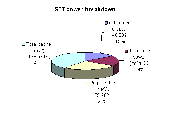
Figure 1 shows the proportion of power consumed by each architectural block. Figure 1 includes the cache memories (total cache is both data and instruction) which assume half reads/half writes every cycle to the instruction cache, and half reads/half writes to the data cache every second cycle (based on instruction mix of 50% load/store operations).
Figure 1 - Power breakdown of LEON2 Processor
As shown in Figure 1, the caches are large consumers of power. The register file is also a large consumer of
power. This is due in part to the SPARC architecture and support of
register
windows and also in part to the implementation. In this design there
are
136 32-bit registers, more than most RISC processors. In this
implementation, the 136 32-bit register memory array is instantiated
twice from the standard cell RAM generators to acheive the
functionality of two simultaneous read ports. Thus, the
implementation of the register file is in effect very large and
consumes a large portion of the power. Figure 2 shows just the core
and clock tree power of the LEON2 Processor
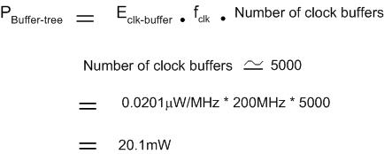
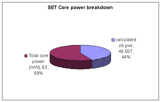 Figure 2 - Power breakdown of LEON2 Processor excluding data and instruction caches Clock Distribution Network calculation details
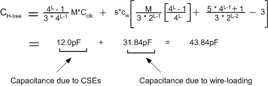
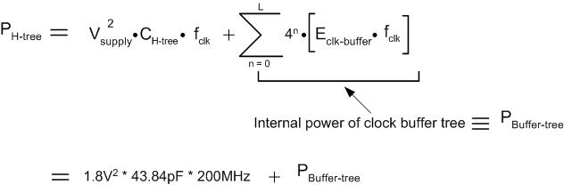
The method for estimating the power consumed in the clock distribution
method is detail in the power analysis
methodology section of the project roadmap. Some of the
equations are reproduced below for convenience. The estimate is
based on the estimated loading of an H-tree distribution network.
The values of the parameters used are detailed below. |
|
|